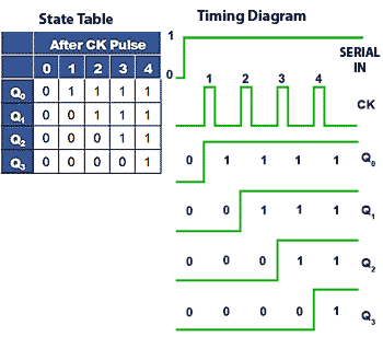
43 register timing diagram
PDF Timing pulse Shift Register A Shift Register B 1997 by Prentice-Hall, Inc. LOGIC AND COMPUTER DESIGN FUNDAMENTALS Simon & Schuster/A Viacom Company Mano & Kime Upper Saddle River, New Jersey 07458 T-103 Timing pulse Shift Register A Shift Register B › coa-register-transferCOA | Register Transfer - javatpoint The following image shows the block diagram that depicts the transfer of data from R1 to R2. Here, the letter 'n' indicates the number of bits for the register. The 'n' outputs of the register R1 are connected to the 'n' inputs of register R2. A load input is activated by the control variable 'P' which is transferred to the register R2.
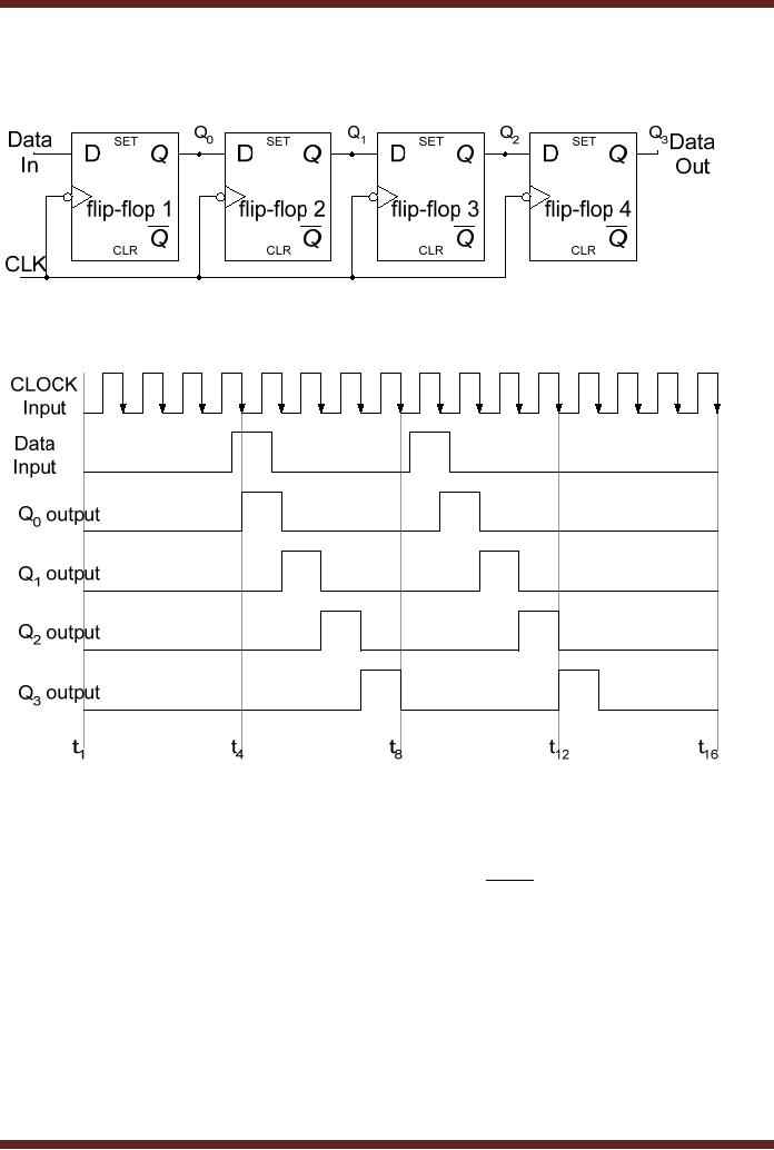
digital logic - Understand the timing of Shift Register ... From the Wikipedia, I found the following diagram about SIPO shift register: As I understand, this shift register is made of DFF (D Flip-Flop). DFF is triggered at the rising edge of the clock period. So for each rising edge of the Clock signal, the data from the Data In will propagate through one stage of DFF.

Register timing diagram
Help me understand this shift register timing diagram On every clock pulse, the state of the serial data pin is read As data is read, it gets shifted in to the registers When the latch pin pulses the values in the register are sent to the parallel output pins Here is a timing diagram for the 74HC595. SH_CP is the clock, and DS is the serial data pin. PDF Shift registers - Griffith University Figure 3.2: The timing diagram of 74HC164 4.0 Parallel In - Serial Out Shift Registers A four-bit parallel in- serial out shift register is shown below. The circuit uses D flip-flops and NAND gates for entering data (ie writing) to the register. PDF Register File Block Diagram - cs.uni.edu Register File Block Diagram: Most register files have at least two read/output ports and one write/input port to accommodate sending two values to the ALU and receiving one result. To control a read port we need to be able to specify a register number for the register to be read. The width/number of bits read equals the number of bits per register.
Register timing diagram. Timing Diagram - an overview | ScienceDirect Topics Timing diagram is a special form of a sequence diagram. The most notable graphical difference between timing diagram and sequence diagram is that time dimension in timing diagram is horizontal and the time is increasing from left to the right and the lifelines are shown in separate compartments arranged vertically. Shift Registers in Digital Electronics - Javatpoint Below is the diagram of 4-bit "bidirectional" shift register where DR is the "serial right shift data input", DL is the "left shift data input", and M is the "mode select input". Block Diagram Operations 1) Shift right operation (M=1) › synchronous-counterSynchronous counter | Types, Circuit, operation and timing ... Dec 03, 2021 · Operation and Timing Diagram. Before going into the operation of the 3-bit synchronous counter, learn how JK flip-flop and T flip-flop operates. Let us assume the initial condition as Q C Q B Q A = 000. The HIGH input is given only to the first flip-flop(TFF 1). Since Q A = Q B = 0, the inputs are 0 for the remaining flip-flops. Thus T A = 1, T ... Register to Register Path - timing diagrams See the timing diagram below. Register to Register Setup Analysis with Clock Frequency at 51MHz Hold Analysis The list below shows the delays and constraints that need to be considered for hold analysis of the path from register 1 to register 2. R1 Clock-to-Q Delay Minimum CL Propagation Delay Minimum R2 Hold Constraint Minimum (3) 
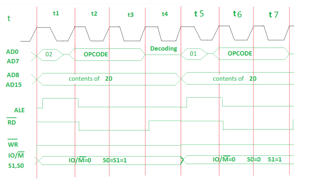
› pin-diagram-8086Pin diagram of 8086 microprocessor - GeeksforGeeks May 17, 2021 · The clock input provides the basic timing for processing operation and bus control activity. Its an asymmetric square wave with a 33% duty cycle. RESET : This pin requires the microprocessor to terminate its present activity immediately. › jk-flip-flopJK Flip Flop: What is it? (Truth Table & Timing Diagram ... Feb 24, 2012 · This is known as a timing diagram for a JK flip flop. In addition to the basic input-output pins shown in Figure 1, J K flip-flops can also have special inputs like clear (CLR) and preset (PR) (Figure 4). circuitdigest.com › tutorial › what-is-shiftWhat is Shift Register? Working, Applications & Types of ... The timing diagram of the device is also shown below. It will better help you understand how the control line controls the actions of the register. 6. Counters Counters, sometimes called rotate shift register are basically shift registers with their outputs fed back into the device as inputs in such a way that it creates a particular pattern. Timing Diagram of OPCODE FETCH - Timing Diagrams and ... The process of data flow and timing diagram of fetch operation are shown in Figs. 3.3 (a), (b), and (c). The µP fetches opcode of the instruction from the memory as per the sequence below • A low IO / M means microprocessor wants to communicate with memory. • The µP sends a high on status signal S 1 and S 0 indicating fetch operation.
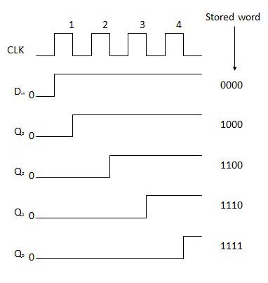
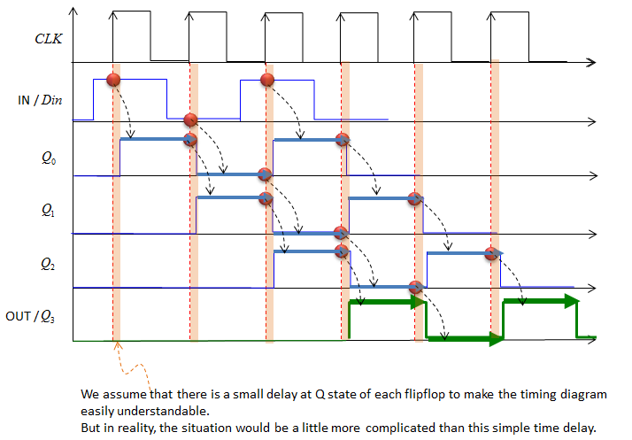
Help me understand this shift register timing diagram ... On every clock pulse, the state of the serial data pin is read As data is read, it gets shifted in to the registers When the latch pin pulses the values in the register are sent to the parallel output pins Here is a timing diagram for the 74HC595. SH_CP is the clock, and DS is the serial data pin. Shift Registers Worksheet - Digital Circuits A shift register circuit is ideal for this application. Shown here is an eight-bit shift register circuit: Draw any necessary wires and labels showing where serial data would enter the circuit, and where parallel data would exit. Reveal answer Question 15 AN-CM-303 8-bit SISO, SIPO, PISO, PIPO Shift Registers ... The timing diagram of the SIPO shift register is shown in Fig 4. It has a clock and Serial Data-in as the first two waveforms, and all other waveforms are the outputs of the DFF's. It can be observed that after the 8 th rising edge of the clock, the entire input data bits are visible at the output of each DFF. PDF D-Register Timing - I D-Register Timing - I CLK D Q D DQ CLK Q t CD t CD: minimum contamination delay, CLK→Q >t SETUP t SETUP: setup time guarantee that D has propagated through feedback path before master closes >t HOLD t HOLD: hold time
What is a Shift Register? Definition, Operation and ...
8085 Instruction Cycle And Timing Diagram ... The timing diagram is a graphical representation of the process in steps with respect to time. It represents the step by step working of each instruction and its execution. The execution time of instructions is represented in T-states. Machine Cycle - The time required to access the memory or input/output device is called the machine cycle.
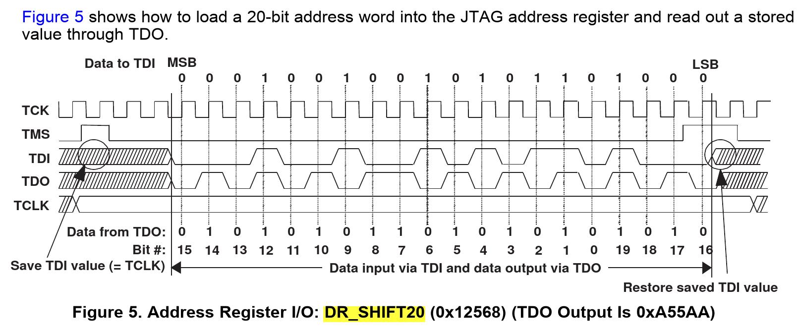
Timing diagram and register contents of the signals and ...
WaveDrom - Digital timing diagram everywhere Digital Timing Diagram everywhere. WaveDrom draws your Timing Diagram or Waveform from simple textual description. It comes with description language, rendering engine and the editor. WaveDrom editor works in the browser or can be installed on your system. Rendering engine can be embeded into any webpage. Download editor Issues User group ...

74LS166 8-bit Shift Register Pinout, datasheet, examples and ...
Timing Diagram Software | Create UML Timing Diagrams ... Create a Timing Diagram Over 8 Million people and 1000s of teams already use Creately Draw timing diagrams with minimal effort Advanced features to simplify creating even the most complex of timing diagrams with amazing ease. Smart shapes and connectors, plus create and multiple diagramming shortcuts.
Catherine on Twitter: "even more cursed timing diagram for ...
Universal Shift Register : Design, Working & Its Applications Universal Shift Register Diagram. Serial input for shift-right control enables the data transfer towards the right and all the serial input and output lines are connected to the shift-right mode. The input is given to the AND gate-1 of the flip-flop -1 as shown in the figure via serial input pin.
Write truth table, timing diagram and logic diagram of SISO ...
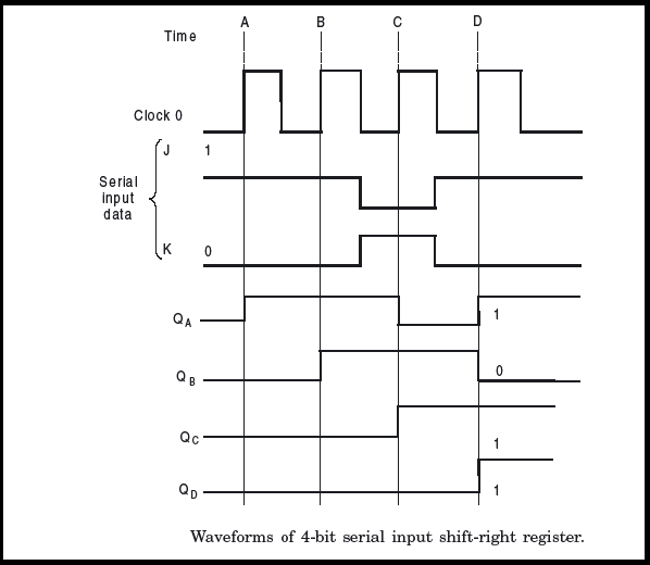
SHIFT REGISTERS:Serial In/Shift LeftRight/Serial Out ... usually shifted in to fill up the vacant bits in the shift register. Figure 34.3a Serial In/Shift Right/Serial Out Register Figure 34.3b Timing diagram of a Serial In/Shift Right/Serial Out Register The shift left and shift right shift registers are identical in their working. They are

CSE370 Assignment 7
Timing diagram of INR M - GeeksforGeeks Timing diagram of INR M. Problem - Draw the timing diagram of the given instruction in 8085, The content present in the designated register/memory location (M) is incremented by 1 and the result is stored in the same place. If the operand is a memory location, it is specified by the contents of HL pair. M is the memory location (say 5000H ...
Refresh and Display Timing - Logisim - BREDSAC
Timing diagram of MVI instruction - GeeksforGeeks Timing diagram of MVI instruction. Explanation of the command - It stores the immediate 8 bit data to a register or memory location. Operand: B is the destination register and 45 is the source data which needs to be transferred to the register. '45' data will be stored in the B register.
Serial-in Serial-out Shift Register (SISO) - InstrumentationTools
Timing Diagram Basics - Rheingold Heavy Timing Diagrams are a way to symbolically represent the activity of one or more signals being transmitted or received by a component, and the way they relate to each other over a span of time. Any device that communicates with other devices over serial communications methods will include them in their datasheet.
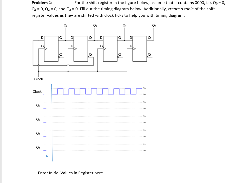
Answered: Problem 1: For the shift register in… | bartleby
How to Read Timing Diagrams: A Maker's Guide | Custom ... As you can see, the timing diagram is an addition to the textual description to make it easier to visualize the operation of the device. Knowing this, let's continue by looking at the counting process. In this example, the counter is preset to twelve: As you can see, the input data was present long before the load operation was triggered.

CMPEN 271 Homework
Timing Diagram Explained | EdrawMax Online Source:EdrawMax Diagram 2: Boat manufacturing process. 4. Conclusion One of the key benefits of a UML timing diagram is that it gives users an overview of what goes on in a system or piece of software. More critically, it shows which steps in a system take too much time, and this information can be used by business users and developers alike to improve their processes.

ATtiny102/ATtiny104 Complete
Register File Timing Diagram - YouTube Example trace of a timing diagram for a register file
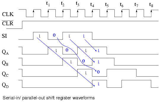
Serial-in, parallel-out shift register : SHIFT REGISTERS
Timing diagrams and Machine cycles - Learn with 8085 ... A timing diagram in the field of embedded systems refers to a graphical representation of processes occurring with respect to time. In other words, the representation of the changes and variations in the status of signals with respect to time is referred to as a timing diagram. Take the below illustration as an example.
Registers
Understanding Timing diagrams of digital systems - Do It ... Timing diagrams are the main key in understanding digital systems. Timing diagrams explain digital circuitry functioning during time flow. Timing diagrams help to understand how digital circuits or sub-circuits should work or fit into a larger circuit system. So learning how to read Timing diagrams may increase your work with digital systems and integrate them. Bellow is a list o most commonly ...

Serial in Parallel Out (SIPO) Shift Register | Electrical4U
› architecture-of-8085Architecture of 8085 microprocessor - GeeksforGeeks Nov 07, 2021 · Instruction register and decoder : It is a 8-bit register that holds the instruction code that is being decoded. The instruction is fetched from the memory. Timing and control unit : The timing and control unit comes under the CPU section, and it controls the flow of data from CPU to other devices.

Register File Timing Diagram
› tutorials › seqrevHow to Generate Sequence Diagram from Java? Nov 10, 2014 · The Create new sequence diagram option is selected and diagram name is entered by default. Click Finish button. As a result, a UML sequence diagram is formed. Let's study the diagram. When a person invokes RegisterController's register method (message: 1), it creates an account object (message: 1.1). After that, the controller sets the id, name ...
Shift Registers Worksheet - Digital Circuits
PDF Register File Block Diagram - cs.uni.edu Register File Block Diagram: Most register files have at least two read/output ports and one write/input port to accommodate sending two values to the ALU and receiving one result. To control a read port we need to be able to specify a register number for the register to be read. The width/number of bits read equals the number of bits per register.

datasheet - Help me understand this shift register timing ...
PDF Shift registers - Griffith University Figure 3.2: The timing diagram of 74HC164 4.0 Parallel In - Serial Out Shift Registers A four-bit parallel in- serial out shift register is shown below. The circuit uses D flip-flops and NAND gates for entering data (ie writing) to the register.
Parallel-in Serial-out Shift Register (PISO ...
Help me understand this shift register timing diagram On every clock pulse, the state of the serial data pin is read As data is read, it gets shifted in to the registers When the latch pin pulses the values in the register are sent to the parallel output pins Here is a timing diagram for the 74HC595. SH_CP is the clock, and DS is the serial data pin.
Shift Registers - Computer Organization And Architecture ...
Shift registers
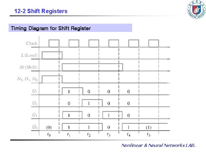
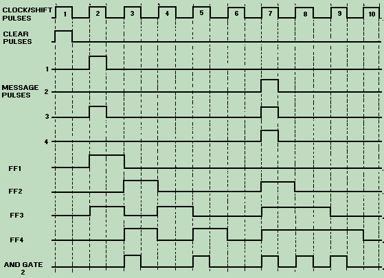
Nonlinear Neural Networks LAB CHAPTER 12 REGISTERS AND

Shift register - Wikipedia
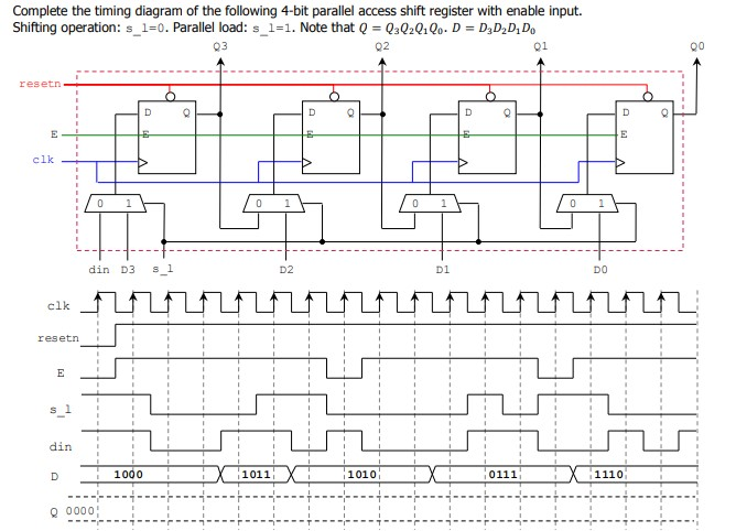
Solved) : Complete Timing Diagram Following 4 Bit Parallel ...
Solved: Need Help Question Anyone Complete Timing Diagram

74HC595 8 bit Shift Register – Zx Lee
Serial in Serial out Shift Register (SISO) | Electronics ...

CSE370 Laboratory Assignment #7

CMPEN 271 Homework

4-Bit Shift Register Timing Diagram Large Image
Timing diagram of MVI instruction - GeeksforGeeks

Output setting time for shift register (74HC595) - Electrical ...
Digital Registers
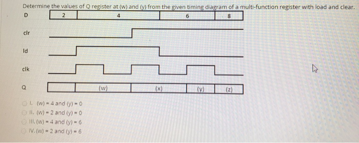
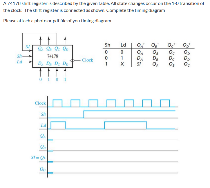
Solved: Determine the values of Q register at (w) and (y)
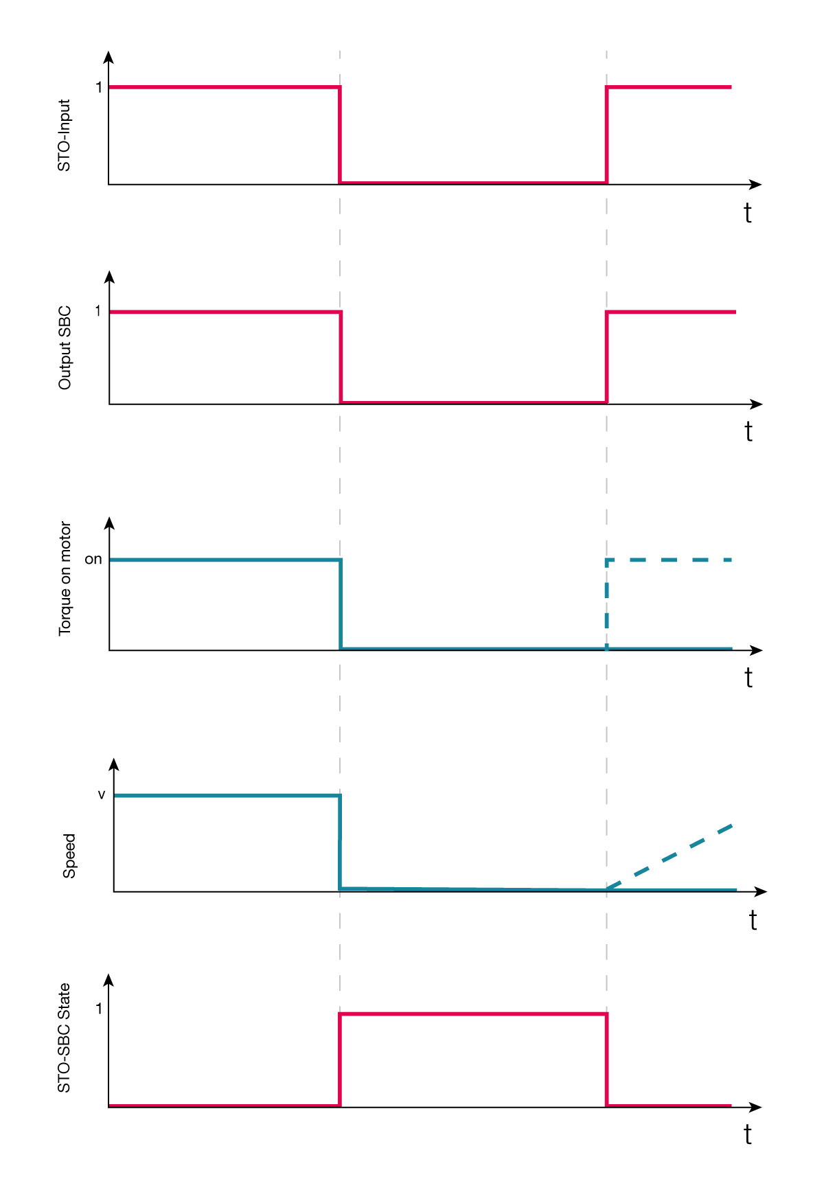
Using the safety functions — Synapticon Documentation
Shift registers
Registers
Click PLC Shift Register Instruction | Acc Automation
State Elements

What is Shift Register? Working, Applications & Types of ...
ShareTechnote
SHIFT REGISTERS:Serial In/Shift LeftRight/Serial Out ...

Smiley's Workshop 28: Gettin' A Little Shifty | Nuts & Volts ...
Solved] A 4x4 register file has 4, 4-bit registers. The ...


Comments
Post a Comment